Description


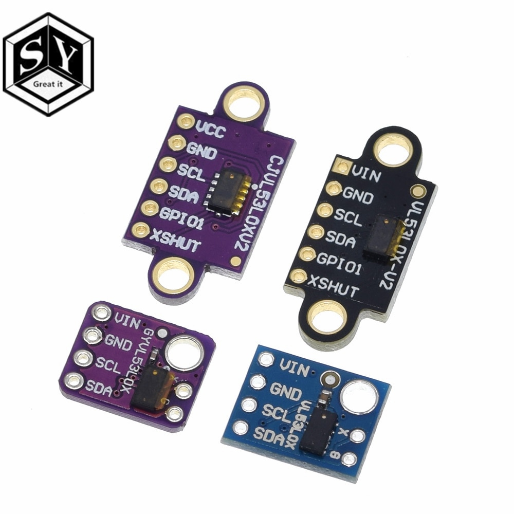
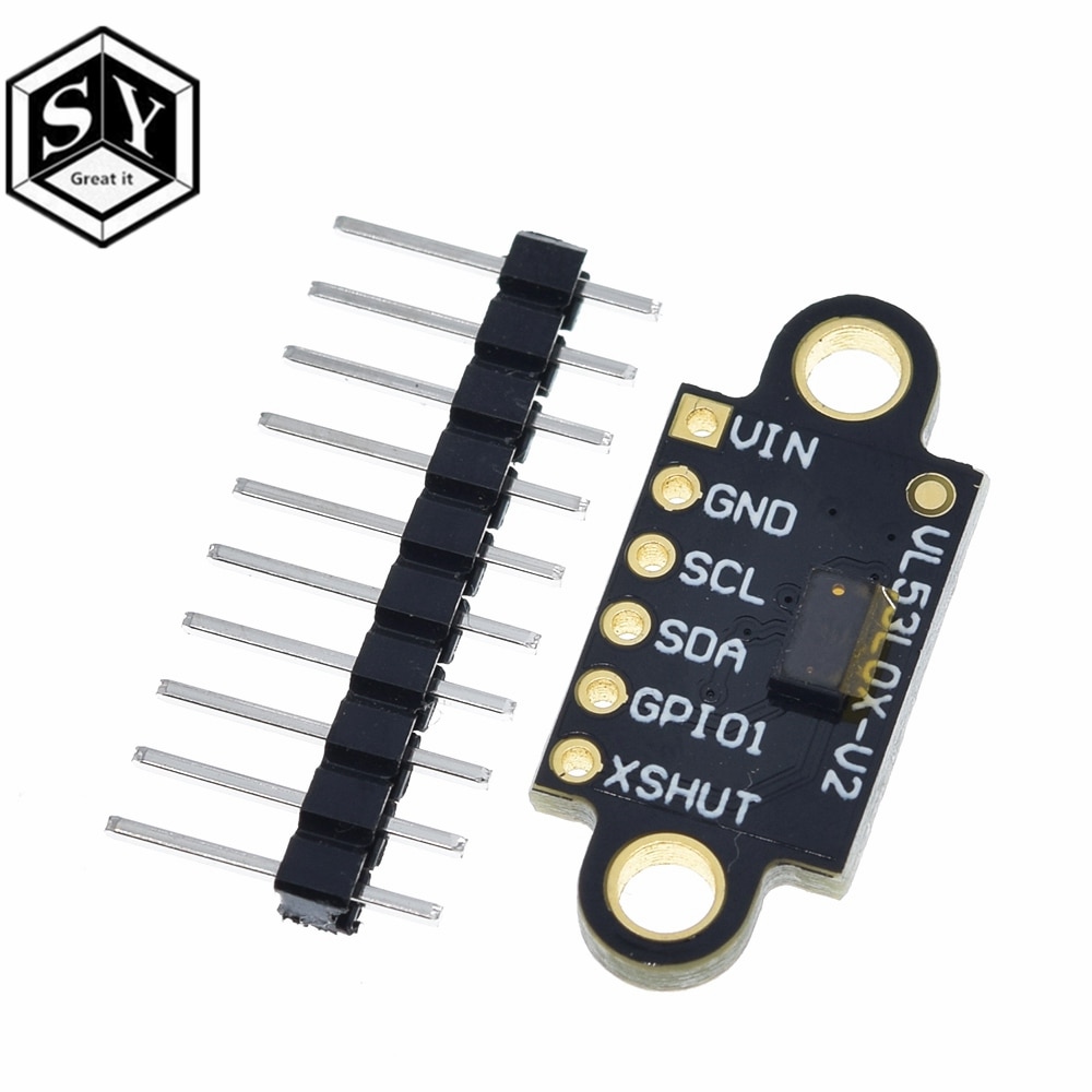
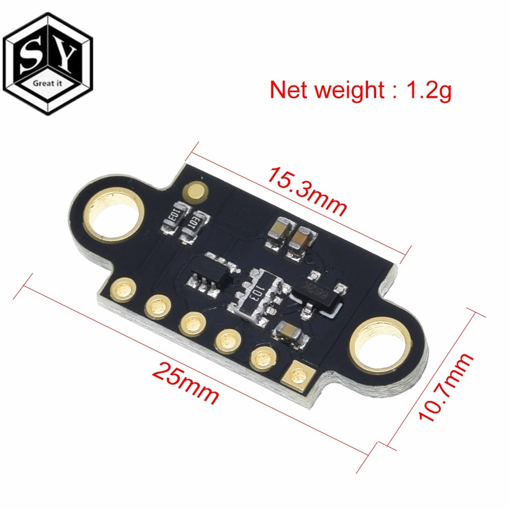
PIN Description
VDD Regulated 2.8 V output. Almost 150 mA is available to power external components. (If you want to bypass the internal regulator, you can instead use this pin as a 2.8 V input with VIN disconnected.)
VDD Regulated 2.8 V output. Almost 150 mA is available to power external components. (If you want to bypass the internal regulator, you can instead use this pin as a 2.8 V input with VIN disconnected.)
VIN This is the main 2.6 V to 5.5 V power supply connection. The SCL and SDA level shifters pull the I2C lines high to this level.
GND The ground (0 V) connection for your power supply. Your I2C control source must also share a common ground with this board.
SDA Level-shifted I2C data line: HIGH is VIN, LOW is 0 V
SCL Level-shifted I2 C clock line: HIGH is VIN, LOW is 0 V
XSHUT This pin is an active-low shutdown input; the board pulls it up to VDD to enable the sensor by default. Driving this pin low puts the sensor into hardware standby. This input is not level-shifted.


