Abstract
Low cost, compact and robust single mode semiconductor laser diodes emitting at λ ∼ 1.6–2.1 μm are highly desirable as light sources for trace gas spectroscopy and an increasing number of other applications, such as, high data-rate communications over hollow core photonic crystal fibre, noninvasive optical blood glucose monitoring. Indium phosphide based light sources provide a solid and flexible base for mid-infrared semiconductor diode lasers. This chapter provides an overview of the current state of the art in discrete mode InGaAs/InP long-wavelength quantum-well lasers emitting in the 1.6–2.1 μm wavelength range. The discrete mode laser is essentially a regrowth free modified ridge waveguide Fabry-Pérot laser whose optical spectrum has a single wavelength mode. High-performance and cost-effective mid-infrared DM laser diode sources are well suited to a wide range of sensor applications. The current state of the art will also be outlined in this chapter.
Keywords
- semiconductor laser
- mid-infrared sources
- single mode laser
- strained quantum-well
- absorption spectroscopy
1. Introduction
Low cost single mode semiconductor laser diodes emitting at wavelengths, λ, in the 1.6–2.1 μm wavelength range are highly desirable as light sources for trace gas spectroscopy due to the strong absorption bands [1] in this spectral region. Compared to conventionally used systems based on electrochemical point sensors, tuneable diode laser absorption spectroscopy (TDLAS) offers a number of benefits for the detection of gases such as; rapid response time, long term stability, high selectivity and sensitivity, rugged systems and measurement capability over long distances using open path systems [2]. TDLAS is based on the molecular rotational-vibrational absorption of gases that produce distinct peaks in the near to mid-infrared (IR) spectral range. These molecule resonances cause characteristic ‘fingerprints’ by selective absorption of laser light as the wavelength is tuned by changing the laser bias current or heat sink temperature. Great interest is due to the strong absorption lines of various important gases, such as methane (1.665 μm), hydrogen chloride (1.743 μm), and nitrous oxide (1.795 μm), in this wavelength range. Two pertinent greenhouse gases, water vapour (H2O) and carbon dioxide (CO2), have strong absorption bands at wavelengths centred around 1.877 and 2.004 μm respectively and are shown in Figure 1. There is also an increasing number of other applications, such as high data-rate communications over hollow core photonic crystal fibre [3, 4, 5, 6] and noninvasive optical blood glucose monitoring [7] which also require compact and robust low-cost laser sources emitting in the 1.6–2.1 μm wavelength range.
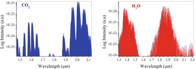
Figure 1.
Absorption spectra of two important greenhouse gases CO2 and H2O, with strong absorption lines in the near-to-mid-IR extracted from the HITRAN database [1].
Semiconductor laser diode materials with light emission in the 1.6–2.1 μm wavelength range include indium phosphide (InP) and the gallium antimonide (GaSb) material systems. It must be noted that cost sensitivity is a significant issue for many of these applications and in order to keep the laser chip cost down the InP material is often preferred over the GaSb material system for emission in the mid-IR region. In comparison with the GaSb material platform, the processing technologies for InP-based materials are more mature as they were developed for telecommunications lasers. In addition, superior substrate quality, lower substrate cost, better thermal performance and mature growth methods make InP-based lasers attractive candidates for light sources in this wavelength region [8, 9, 10, 11, 12, 13, 14, 15]. The III-V compound semiconductor material system (AlGaIn)-(AsP) constitutes an ideal basis for the realization of diode lasers in this wavelength region [16]. InGaAs, either lattice matched to InP or deliberately strained, can be used for the active layer with a direct band gap between 1.1 and 2.3 μm. Recently InP-based type-II QWs have extended the wavelength up to 3 μm [17] which opens up another important wavelength region for the fabrication of lower cost lasers for sensing applications.
This chapter begins with an overview of mid-IR single mode laser diodes and then outlines the state of the art in InP based mid-IR discrete mode laser diodes.
2. Overview of the state of the art in mid-IR single mode laser diodes
In this section an overview of the current state of the art in compact monolithic single mode laser diodes emitting in the 2.0 μm spectral region will be outlined. Focusing on monolithic chips, external cavity laser devices are not included here. The review will start with an overview of the material systems available for the laser active region emission in the 2 μm spectral region. To date single mode semiconductor lasers have been demonstrated in both the GaSb and indium InP material systems. Both material systems have their pros and cons and an overview of the various technology implementations for achieving single wavelength mode operation in each material system is shown.
2.1 Gallium antimonide (GaSb) laser diodes
The III-V compound semiconductor material system (AlGaIn)(AsSb) constitutes an alternative basis for the realisation of diode lasers in the mid-IR. GaInAsSb is either latticed matched to GaSb substrates or strained and is used as the active layer with a direct bandgap transition covering the λ ∼ 1.8–3.4 μm wavelength region. For the barrier and cladding layers, AlGaAsSb is well suited because of its larger bandgap energy and lower refractive index compared to GaInAsSb. Molecular-beam epitaxy (MBE) is the method of choice and most widely used in the wafer growth. The laser structures are grown on (100)-orientated n-doped GaSb substrates but due to the lower demand for GaSb substrates compared to InP the growth cost is higher and substrate quality lower. Conventional fabrication of distributed-feedback (DFB) lasers incorporating buried gratings for longitudinal mode selection is challenging in the GaSb material system due to the difficulty of epitaxial regrowth with the high Al concentrations in the cladding layers. Separately, processing options are quite limited for GaSb due to the cladding material being hygroscopic.
2.1.1 Laterally coupled distributed-feedback
A proposed method for DFB fabrication which was recently demonstrated by the Jet Propulsion Laboratory (JPL) [18], makes use of Bragg gratings etched alongside a ridge waveguide to form a laterally coupled distributed-feedback (LC-DFB) as shown in Figure 2This approach enables fabrication of single-longitudinal-mode laser following a single epitaxial growth process.
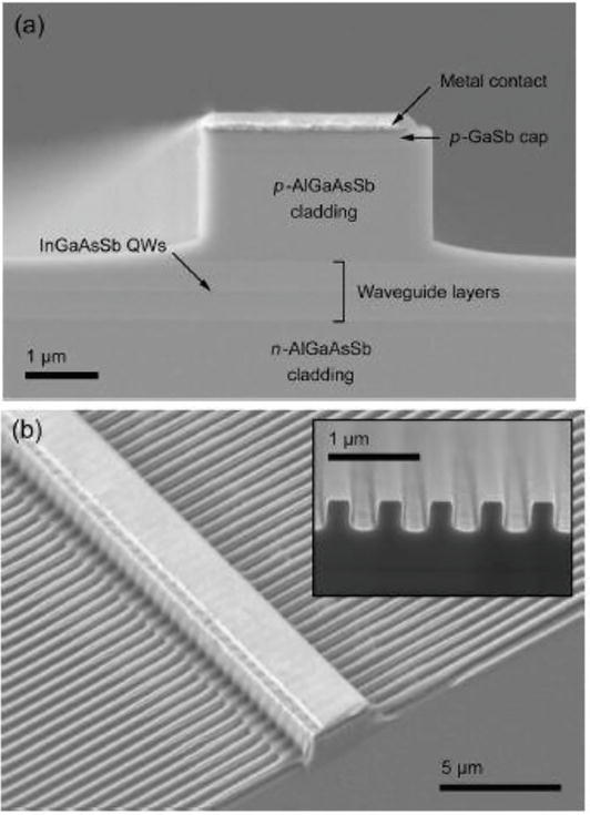
Figure 2.
(a) Cross-section scanning-electron micrograph of a 3-μm-wide laser ridge topped with a titanium-platinum-gold contact layer. (b) Top view of the LC-DFB laser structure, with a cross section of the grating (inset) [18].
Characteristics of the LC-DFB laser are as follows; at a heat sink temperature of −10°C they demonstrate a single mode emission in the 2054 nm region with an SMSR > 30 dB and ex-facet power exceeding 80 mW. This is the highest reported power from a DFB laser at 2 μm. The wavelength shift with current and temperature is reported to be 5.39 × 10⁻³ nm/mA and 0.2 nm/oC [19]. They also demonstrated LC-DFB laser linewidths of 1.4 MHz and 900 kHz for 500 and 10 ms observation times, respectively. The linewidths were derived from the frequency-noise power-spectral density measured using a Fabry-Perot interferometer.
2.1.2 Lateral metal grating DFB
Ridge waveguide GaSb DFB lasers have also been fabricated by the University of Wurzburg and commercialised by the German company NanoPlus which employ a lateral metal grating at the side of the ridge [20] as depicted in Figure 3. The metal gratings provide strong feedback but generate additional absorption loss in the laser cavity hence the ex-facet laser power is limited to ∼10 mW levels.
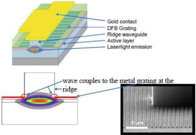
Figure 3.
Schematic diagram of the ridge waveguide metal grating DFB [20].
A single mode emission at 2 μm with a side mode suppression ratio of 31 dB is demonstrated in [20] and output power in the 8 mW region. The wavelength tuning rate with temperature is 0.2 nm/oC. Reported linewidth measurements are in the 0.3–0.5 MHz region [21].
2.2 Indium phosphide (InP) laser diodes
To extend the emission wavelength from λ ∼ 1.55–2.1 μm in the InxGa1-xAs material system compressive strain is applied by increasing the indium (In) composition. Figure 6 shows the calculated bandgap wavelength (λg (μm) = 1.2407/Eg (eV)) for a bulk InxGa1-xAs layer on InP as a function of In composition. As shown in Figure 2, a compressive strain larger than 1% is required to obtain a bandgap wavelength longer than 2 μm. Also shown in Figure 4 is the experimentally measured quantum well photoluminescence peak wavelength for four separate active regions with the In composition varied. When a quantum well structure is used instead of a bulk layer, the bandgap wavelength becomes smaller because of the quantum size effect on the bandgap energy. Therefore larger strain is required for InxGa1-xAs quantum wells (QWs) to obtain the same bandgap wavelength as bulk InxGa1-xAs [14].
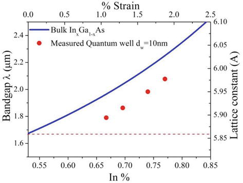
Figure 4.
Calculated bandgap wavelength for InGaAs on InP as a function of In composition. The upper horizontal axis shows the mismatch strain of InGaAs with respect to InP. Red dashed line indicates the lattice constant of InP 5.869A [13].
2.2.1 InP-DFB
InP-based DFB lasers have been extensively developed with wavelengths at 1.3 and 1.55 μm for fibre optic communications over the last three decades. Similar processing techniques can be used for fabrication of single mode lasers operating in the 2 μm wavelength range. NTT-Japan demonstrated a DFB laser with an emission wavelength of 2.051 μm and output power of 10 mW [22]. A schematic of their buried heterostructure DFB grating is shown in Figure 5. The DFB grating was buried and required two regrowth stages after grating formation. There are no reported measurements on the spectral linewidths but they are expected to be in the 2 MHz range. The ex-facet power of 10 mW was improved on in a subsequent paper [23] with a value of ∼20 mW reported. The wavelength shift with current and temperature is reported to be 0.0025 nm/mA and 0.125 nm/oC [24].
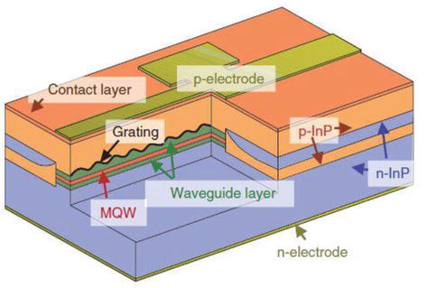
Figure 5.
Schematic of BH-DFB laser diode [23].
2.2.2 Vertical-cavity surface-emitting laser
Light propagation and emission normal to the semiconductor layer structure is characteristic of a vertical-cavity surface-emitting laser (VCSEL) [25]. The main feature of the VCSEL design is the regrown buried tunnel junction (BTJ) (see Figure 6), which accomplishes current confinement and wave guiding. The active region contains five heavily compressively strained InGaAs-quantum wells separated by tensile strained barriers of InGaAIAs. Current is injected through a contact pad on the epitaxial mirror and the gold heat sink via the n + doped contact layers [25]. The n-doped epitaxial mirror reflectivity of the front mirror of 99.4% and back mirror reflectivity was 99.9%. The dielectric DBR is combined with an integrated electroplated Au-heat sink and a buried tunnel junction. VCSEL’s emitting in the 2 μm region have been demonstrated by the Technical University Munich and commercialised by VERTILAS in the InP material system [25] however the ex-facet power levels from this technology is limited to <1 mW. Due to the very short laser cavity spectral linewidths from VCSEL devices are typically >20 MHz [26], and show high tuning rates of 0.67 nm/mA and 1.5 nm/oC.
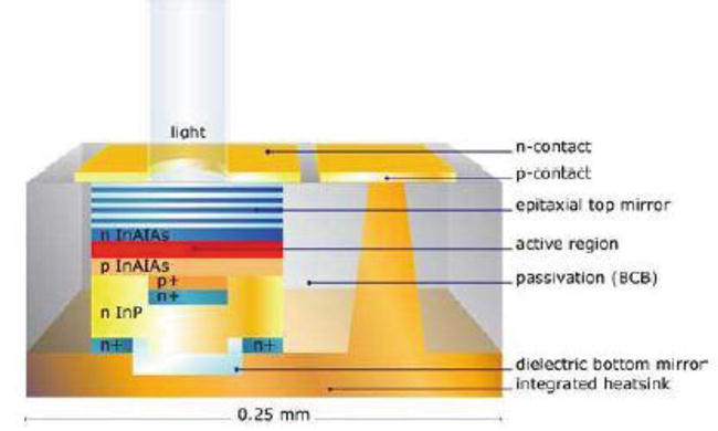
Figure 6.
Schematic of VCSEL laser diode [26].
2.2.3 InP-discrete mode laser diode
Discrete mode (DM) technology is Eblana Photonics proprietary method of manufacturing single mode lasers. Single wavelength operation in DM lasers is achieved by introducing index perturbations in the form of etched features positioned at a number of sites distributed along the ridge waveguide laser cavity as shown in Figure 7. Eblana has recently fabricated single mode lasers in the 2 μm spectral region [13]. The spectral linewidths for DM laser emitting at 2.0 μm is 1 MHz. The ex-facet power of 5 mW was measured and the wavelength shift with current and temperature is reported to be 0.0025 nm/mA and 0.125 nm/°C [13].
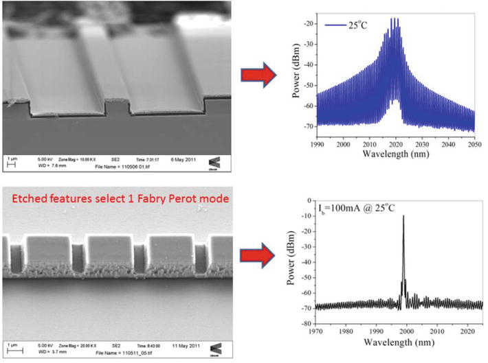
Figure 7.
Electron micrograph of Fabry Perot laser cavity (top left) and DM laser, fabricated by etching slots into laser ridge (bottom left) along with spectral characteristics of typical mid-IR laser with and without etched features (top and bottom right respectively).
3. Mid-IR DM laser
3.1 Design of InP ridge waveguide FP lasers
A typical InP based Type-I laser structure for an emission wavelength of 1.6–2.1 μm is shown in Figure 8 [14]. For most of the laser structures reported on in Section 3, two to three compressively strained QWs are used as the active region with a width of 10 nm. They are separated by 15–30 nm thick InxGa1-xAs barrier layers which are either lattice matched to the InP substrate or tensile strained in order to reduce the average strain in the active region. The active region is sandwiched between two 200 nm-thick InGaAsP separate confinement guide layers with a bandgap wavelength of λg = 1.3 μm which also acts as an etch stop layer for ridge waveguide definition. A 1800 nm thick p-InP layer is grown on top of the separate confinement heterostructure followed by a 200 nm thick highly p-doped InxGa1-xAs contact layer [3].
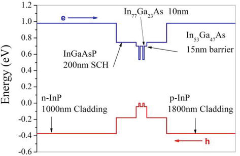
Figure 8.
Direct bandgap profile of an InP-based type-I laser structure with an emission wavelength of 2.1 μm [14].
For the results shown below, four laser structures with varying In compositions were grown on 75 mm diameter n-type (100)-InP substrates in a metal-organic vapour-phase epitaxy reactor at low pressure. The overlapped photoluminescence spectra for the four wafers are shown in Figure 9 measured at room temperature. The sharp peaks indicate high material quality with low defects.
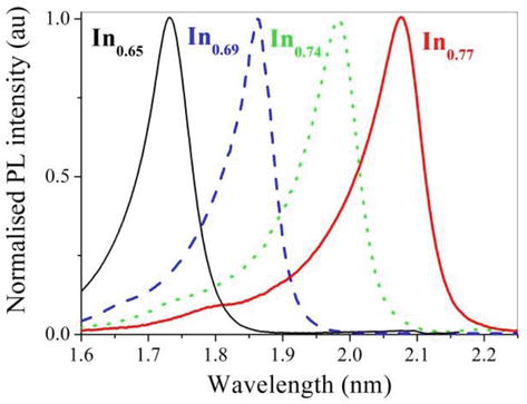
Figure 9.
Overlapped measured photoluminescence spectra at 25°C for four wafers with varying In composition.
The optical waveguiding properties of the ridge waveguide structure was determined by carrying out 2-D numerical simulations and one example for the 2 μm wafer (In = 0.74) is shown in Figure 10. The modal analysis of the structure showed that no higher order lateral modes are supported when the ridge width is 2 μm and that the calculated effective index for the waveguide is 3.2. This effective index is used to calculate the grating pattern spacing required to give single mode emission at the target wavelength which will be described below [3].
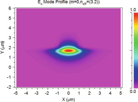
Figure 10.
2D simulation of a ridge waveguide laser diode.
3.1.1 FP laser fabrication
In order to make good single longitudinal mode lasers, the ability to fabricate uniform, highly reliable FP lasers is essential and complete wafers of FP lasers were processed for material evaluation. For the laser to operate in a single lateral mode, control of the ridge width is critical. Simulations showed that a 2 μm wide ridge results in a stable transverse mode. The waveguide was realised using inductive coupled plasma dry etching, the dry etch chemistry used was Cl/N2 followed by a short wet-etch to remove surface roughness. Electrical contacting was achieved using conventional metals (Ti/Pt/Au) and SiO2 as an insulator for contact definition on the heavily doped (p ∼ 2 × 1019 cm−3) p+-InGaAs capped layer. A scanning electron microscope (SEM) image of the fabricated ridge waveguide is depicted in Figure 11a. Finally the wafers were thinned to 150 μm by mechanical polishing and the n-metal electrode applied [3]. A completed wafer is shown in Figure 11b. Subsequently bars were cleaved into 900 μm cavity lengths and the front and back facets coated 20 and 95% respectively.
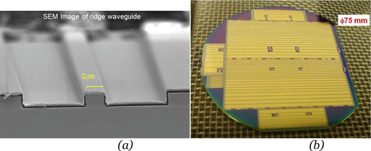
Figure 11.
(a) SEM image of a ridge waveguide FP laser diode. (b) Picture of a processed 3-inch InP wafer.
3.1.2 Mid-IR FP laser characterization
To evaluate the material quality before fabricating the DM lasers, broad area and FP lasers with varying cavity length were fabricated and characterised on the four wafers, only the results from the 2 μm wafer are presented in this section. As-cleaved broad area lasers with 50 μm wide ridge widths and varying cavity lengths were analysed under pulsed conditions (1 μs pulses with 0.1% duty cycle) to evaluate the material quality. The threshold current density (Jth) for the 1000 μm cavity length was 358 A/cm2 (∼119 A/cm2/QW) indicating good material quality. The slope efficiency variation with cavity length allowed the internal quantum efficiency (ni) and the internal optical loss (ni) to be estimated to be 80% and 8 cm−1respectively.
A 600 μm long FP ridge waveguide laser was packaged in a fiberised 14-pin butterfly module which contained a thermoelectric cooler and thermistor and the optical characteristics were measured under CW conditions. Figure 12 shows the overlapped CW measurement of light-current (LI) characteristics measured at chip temperatures 10, 25, 45, 50, 60 and 70°C. The power was measured with a large area (Ø3 mm) extended wavelength InGaAs detector (GPD 3000). The light coupling efficiency into the fibre was measured to be 60% and the chip ex-facet power was >20 mW at 200 mA, 25°C. The extracted threshold currents were 18, 30 and 58 mA at 25, 50 and 70°C respectively. The characteristic temperature of threshold current between 25–50 and 25–70°C was calculated to be 49 and 38 K. The measured slope efficiencies in the fibre at 25 and 50°C were 0.08 and 0.06 W/A respectively [3].
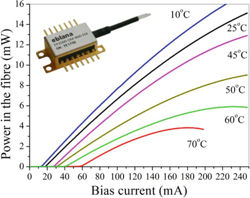
Figure 12.
Overlapped light-current curves in the temperature range 10–70°C for the 2 μm FP laser.
In Figure 13 the emission spectrum is plotted at a heat sink temperature of 25°C and bias current of 80 mA using a Yokogawa (AQ6375) long wavelength optical spectrum analyser. In Figure 14 we overlap the measured optical spectra over a temperature range from 15 to 50°C, the centre lasing wavelength shows a linear dependence with temperature with a tuning rate Δλ/ΔT of ∼0.83 nm/oC, which is consistent with that expected due to the temperature-induced change in the refractive index.
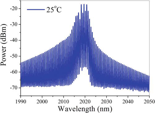
Figure 13.
Emission spectrum at a bias current of 80 mA and heat sink temperature of 25°C.
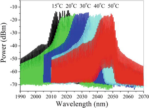
Figure 14.
Overlapped emission spectra at a bias current of 80 mA in the temperature range 25–50°C.
To demonstrate the wide wavelength coverage from 1.65 to 2.15 μm ∼400 nm we overlap the FP emission spectrum for the four wafers as shown in Figure 15.
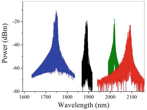
Figure 15.
Overlapped FP emission spectra at bias currents of 80 mA and heat sink temperature of 25°C for the four InP wafers.
3.2 Design of DM laser diodes
Single wavelength operation in DM laser diodes is achieved by introducing index perturbations in the form of shallow-etched features, or slots, positioned at a number of sites distributed along the ridge waveguide as shown in Figure 16a [27, 28, 29, 30, 31, 32]. The slots are realized using ICP dry etching, with a typical depth in the region of 1.5–2 μm and a width of ∼1 μm. The slots are relatively shallow and are not etched into the active (wave guiding) region, however, they will still interact with the mode’s electric field as the mode profile is not fully confined to the active region and will expand into the surrounding cladding regions. This interaction results in a proportion of the propagating light being reflected at the boundaries between the perturbed and the unperturbed sections. In effect the slots act as reflection centres and through suitable positioning the slots manipulate the mirror loss spectrum of an FP laser so that the mirror loss of a specified mode is reduced below that of the other cavity modes [27, 28, 29, 30, 31, 32]. Using a simplified model, developed in [33, 34], a slot can be described as a one dimensional discontinuity inserted into the cavity; as most of the reflection comes from the front of the slot interface. Figure 16b shows a schematic of a laser cavity with slots introduced into the cavity; where rs is the slot reflectivity, ts is the slot transmission, N is the number of slots, L is the distance between the slots, and ϒi is the reflectivity in a section of the cavity where i is the slot number. The reflectivity from the first slot, ϒ1 is given by rs. The introduction of a slot into the waveguide changes its effective refractive index, so that it differs slightly from the segments of the waveguide without slots. The reflectivity from the waveguide to slot interface can be approximated using Eq. (1):
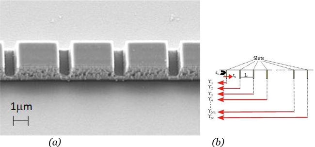
Figure 16.
(a) SEM image of 2 μm wide ridge waveguide with etched grating. The slot width is 1 μm and the spacing between the slots L is 4 μm in this example. (b) Illustration of slot reflection and transmission for N slots.
where n1 is the effective refractive index of the waveguide and n2 is the effective refractive index of the waveguide with a slot.
Assuming no loss from the slot Eq. (2),
ϒ2 is the reflectivity from the second slot and is given by Eq. (3)
where β is the complex propagation constant, and the term ts is squared to take account of forward and backward travelling waves. The exponential term describes the medium in which the light travels, and a factor of two is used again to take account of forward and backward travelling waves. The complex propagation constant takes account of the gain and loss in the transmission medium and is defined in terms of Eq. (4)
where n is the refractive index, λ is the wavelength, g is the optical gain and αi is the internal cavity loss. The reflectivities of the third and fourth slots are given by Eq. (5):
and Eq. (6),
respectively; therefore, the reflectivity obtained from four slots is given by Eq. (7):
By letting Eq. (8)
the total reflectivity from N slots can be expressed by Eq. (9) the following series.
Which in terms of known variables can be described as Eq. (10)
The power reflection is related to the reflection amplitude by Eq. (11),
Using this model the power reflection versus etched feature number at a wavelength of 1887 nm was simulated and shown in Figure 17.
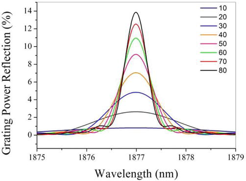
Figure 17.
Simulated power reflection spectrum as a function of slot number.
For a 600 μm long laser cavity at about 60 slots the peak reflectivity begins to saturate and the FWHM is about 0.9 nm which is equivalent to the FP mode spacing. So this is the optimum number of slots for this cavity length.
3.2.1 DM laser fabrication
The fabrication of the DM laser is exactly the same as the FP laser outlined in Section 3.1.2 width the addition of one extra dry etching step to etch the grating, the dry etch chemistry used again was Cl/N2 and was followed by a short wet-etch to remove surface roughness from the grating. A schematic of the etched features is shown in Figure 18.
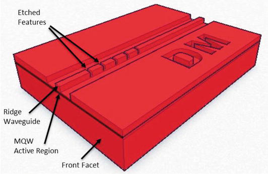
Figure 18.
Schematic view of the InP DM laser.
3.2.2 DM laser diodes emitting at 1.87 μm
Low cost single mode semiconductor laser diodes emitting at 1.87 μm are highly desirable as light sources for trace gas sensing of H2O. The measurement of H2O is important in many industrial applications, for example, continuous emission monitoring in combustion processes where the vapour concentration can be related to performance parameters, such as, efficiency of combustion and heat release. In this section we present data on DM laser diodes operating around λ = 1.877 μm. Fabricated DM lasers exhibit continuous wave (CW) mode hop free operation in the temperature range from 15 to 55°C with emission wavelengths centred at 1.87 μm at 25°C, and ex-facet optical output power >3 mW at 25°C.
A ridge waveguide 600 μm in length DM laser diode was die bonded to an aluminium nitride submount and the optical characteristics were measured under CW conditions. Figure 19 plots the overlapped CW measurement of ex-facet LI characteristics measured at chip temperatures of 15, 25, 35, 45 and 55°C, with the same power and wavelength measurement setup as mentioned in the previous section. The extracted threshold currents were 12, 15, 18, 22 and 29 mA at 15, 25, 35, 45 and 55°C, respectively. The measured slope efficiencies at 15 and 55°C were 0.038 and 0.022 W/A, respectively.
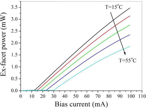
Figure 19.
Overlapped CW LI curves as a function of heat sink temperature.
In Figure 20 the emission spectrum of the DM laser diode is measured at a heat sink temperature of 25°C and bias current of 100 mA. A peak wavelength of 1877 nm is demonstrated, with a side mode suppression ratio (SMSR) of ∼45 dB achieved, in excellent agreement with simulated values. In Figure 21a we plot the peak wavelength versus bias current as a function of laser submount temperature. The peak wavelength tunes linearly with bias current at a tuning rate of ∼0.017 nm/mA. In Figure 21b the optical emission spectrum over a wide temperature range, from −5 to 55°C, is plotted. The single mode peak lasing wavelength shows a linear dependence with current and temperature, with a tuning rate of Δλ/ΔI ∼0.017 nm/mA and Δλ/ΔT of 0.113 nm/oC, consistent with that expected due to the temperature-induced change in the refractive index [29].
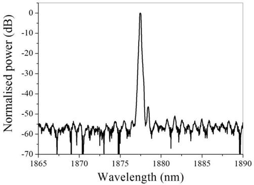
Figure 20.
Normalised optical emission spectrum at a bias current of 100 mA and heat sink temperature of 25°C with SMSR >45 dB demonstrated.
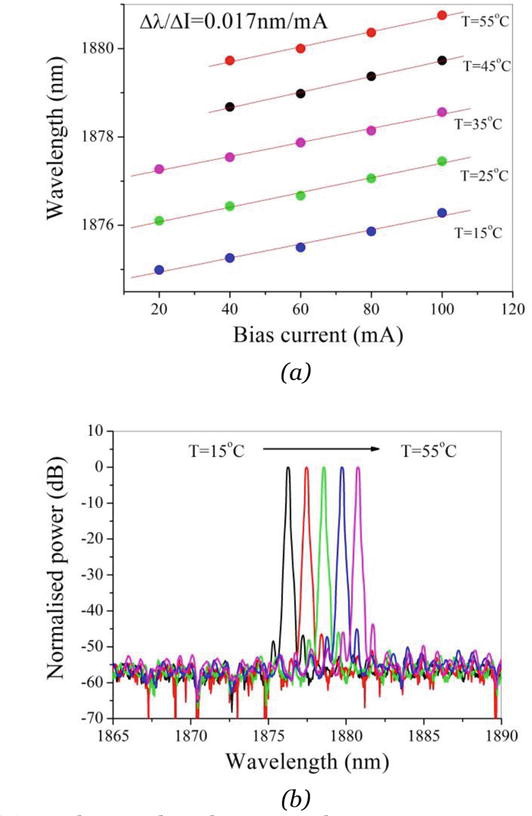
Figure 21.
(a) Peak wavelength versus bias current over temperature. (b) Overlapped optical emission spectra versus heat sink temperature at a fixed laser bias current of 100 mA.
Wide gain bandwidth is demonstrated in Figure 22 where the DM peak wavelength is varied by changing the grating period wavelength tunability of 120 nm is achieved. This makes this material promising for widely-tunable mid-infrared single-mode devices such as DM arrays, external cavity lasers and sampled gratings. Eblana’s DM technology has been used to demonstrate single frequency lasers with high side mode suppression ratios spanning a wide wavelength range from 1.75 to 2.1 μm by using the appropriate InGaAs quantum well composition and thicknesses as shown in Figure 23.
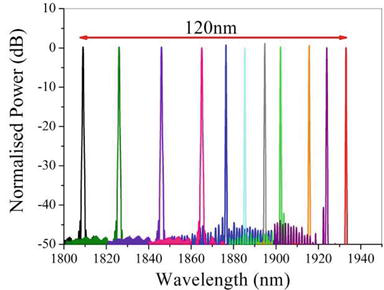
Figure 22.
Overlapped single frequency spectra of 10 different DM lasers demonstrating 120 nm wide gain for the 1.8 μm wafer.
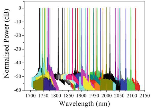
The wavelength and tuning results demonstrated by DM lasers in this chapter show that the devices operate at a single wavelength with SMSR >40 dB robustly over current and temperature variations and, furthermore, that these devices are highly suitable as low cost sources for TDLAS and other sensor applications. A further important feature of the DM laser diode is that its fabrication is far less complex than that of a distributed feedback laser diode resulting in a significant cost advantage.
4. Conclusion
In this chapter an overview in the current state of the art in mid-IR single mode lasers was presented and a low cost laser technology platform based on the InP material system for the manufacture of single mode laser diodes in the near to mid-IR wavelength range introduced. These DM lasers, are ridge waveguide Fabry Perot lasers whose emission spectra have been modified to produce a single mode operation. This modification is achieved during wafer processing by etching surface features into the ridge of an otherwise conventional ridge waveguide laser diode structure and therefore avoiding the need for grating overgrowth [35].
The basic principles underlying DM laser operation and their fabrication have been described. Basic static characteristics of the devices have been discussed and operation in the 1.6–2.1 μm spectral window demonstrated. The results demonstrate that InP-based light sources provide a promising concept for mid-infrared semiconductor diode lasers and are suitable for a range of sensor and other applications.
InP based diode lasers covering the 1.8–2.1 μm range have already reached a considerable level of maturity, as evidenced by the low threshold currents and good spectral performance as highlighted in Section 3. Thus current R&D focuses on the optimization of these lasers towards longer wavelengths >2.3 μm where specific application are in high demand.
This work was supported in part by the European project MODEGAP (FP/2007-2013 under grant agreement 258033) and by the European Space Agency (ESA) under contract reference ESTEC/ITT AO/1 7204/12/NL/NA.

